제품
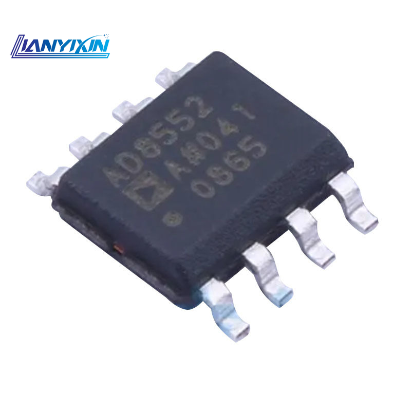
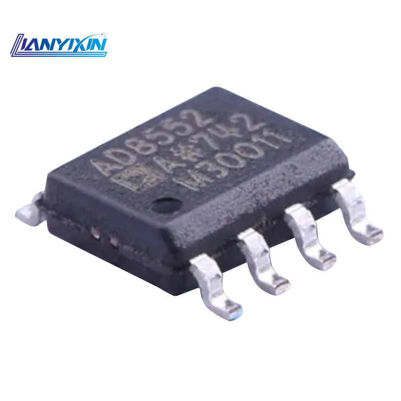
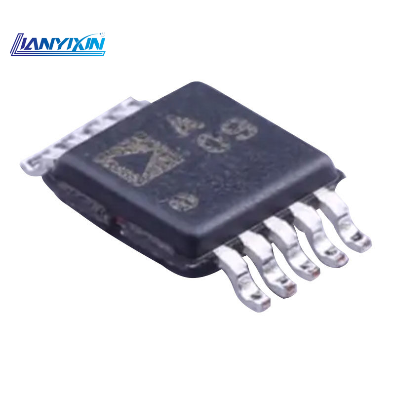
AD8557ARZ-REEL7
AD8557ARZ-REEL7 · Analog Devices (ADI) · 집적 회로
제품 정보
- 부품 번호:
- AD8557ARZ-REEL7
- 증폭기 수:
- 단일 채널
- 입력 바이어스 전류 (Ib):
- 18nA
견적 요청
가격, 재고 및 납기는 견적서에서 확인합니다.
견적 요청기술 사양
동일 모델 · 일관된 매개변수
제품 식별 정보
| 매개변수 | 값 |
|---|---|
| 시리즈 | AD8557ARZ-REEL7 |
전기적 특성
| 매개변수 | 값 |
|---|---|
| 증폭기 수 | 단일 채널 |
| 입력 바이어스 전류 (Ib) | 18nA |
| 입력 오프셋 전압 (Vos) | 2μV |
| 동상 모드 제거비 (CMRR) | 85dB |
| 출력 전류 | 25mA |
| 정지 전류 (Iq) | 1.8mA |
| 단일 전원 | 2.7V – 5.5V |
| 최대 전원 전압 차 (Vdd−Vss) | 5.5V |
| 입력 오프셋 전류 (Ios) | 4nA |
| 동작 온도 | -40°C – +125°C |
패키지 및 기계 사양
| 매개변수 | 값 |
|---|---|
| 이득 대역폭 곱 | 2MHz |
일치하는 매개변수가 없습니다
해당 모델의 매개변수입니다. 패키지와 시험 조건은 제조사 데이터시트를 확인하세요.
원본 항목 · 영어 · 3
일부 원본 항목은 번역 대기 중이며 아래에 영어로 별도 표시됩니다.
| Product Catalogue | Precision Operational Amplifiers |
|---|---|
| Input Offset Voltage Temperature Drift (Vos TC) | 65nV/℃ |
| Noise Density (eN) | 32nV/√Hz @ 1kHz |
제품 개요
번역된 개요가 아직 없습니다. 아래에 해당 모델의 매개변수가 표시됩니다.
영어 원본 보기
Product Overview The AD8557 is a zero-drift sensor signal amplifier featuring digitally programmable gain and output offset capabilities. This amplifier is designed to effortlessly and precisely convert variable pressure sensor and strain bridge outputs into defined output voltage ranges, whilst also accurately amplifying numerous other differential or single-ended sensor outputs. Employing proprietary low-noise auto-zero and DigiTrim technology, the AD8557 delivers a precise and flexible signal processing solution within a compact package. Gain can be digitally programmed over a wide range from 28 to 1300 via a serial data interface. Gain adjustment is fully simulated in-circuit before being permanently programmed using reliable polysilicon fuse technology. The output offset voltage is similarly digitally programmable and proportional to the supply voltage. Beyond its exceptionally low input offset voltage, input offset voltage drift, and extremely high DC and AC common-mode rejection ratios (CMRR), the AD8557 incorporates a pull-up current source at the input pins and a pull-down current source at the VCLAMP pin. Output clamping via an external reference voltage enables the AD8557 to safely and accurately drive low-voltage analogue-to-digital converters (ADCs). When used with an ADC sharing the same supply as the reference, system accuracy remains unaffected by normal supply voltage variations. Output offset voltage adjustment resolution is better than 0.4% of the difference between VDD and VSS. Locking fine-tuning after gain and offset adjustment further ensures field reliability. The AD8557 operates over a temperature range of -40°C to +125°C. This device is powered by a single supply voltage ranging from 2.7 V to 5.5 V and is available in an 8-pin SOIC and a 4 mm × 4 mm, 16-pin LFCSP package. Product Features Ultra-low offset voltage: Maximum 12 μV across the entire temperature range Ultra-low input offset voltage drift: Maximum 65 nV/°C High common-mode rejection ratio: Minimum 96 dB Digitally Programmable Gain and Output Offset Voltage Gain range from 28 to 1300 Compliant with automotive application requirements Single-bus serial interface Stable with any capacitive load SOIC and LFCSP packages Operating voltage range from 2.7 V to 5.5 V Applications Automotive sensors Pressure and position sensors Precision current sensing Thermocouple amplifiers Industrial scales Strain gauges