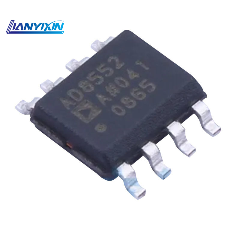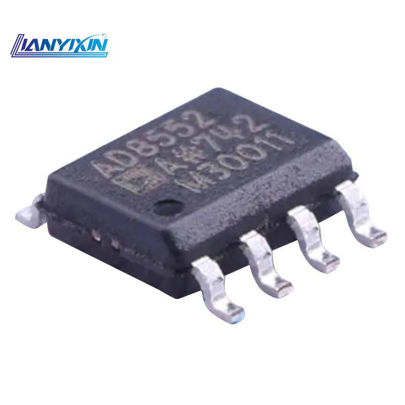
製品
AD8556ARZ-REEL
AD8556ARZ-REEL · Analog Devices (ADI) · 集積回路
製品情報
- 型番:
- AD8556ARZ-REEL
- アンプ数:
- シングルチャンネル
- 入力バイアス電流(Ib):
- 49nA
見積もり依頼
価格、在庫、納期は見積もり時に確認いたします。
見積もり依頼技術仕様
同一型番・一貫したパラメーター
製品識別情報
| パラメーター | 値 |
|---|---|
| シリーズ | AD8556ARZ-REEL |
電気的特性
| パラメーター | 値 |
|---|---|
| アンプ数 | シングルチャンネル |
| 入力バイアス電流(Ib) | 49nA |
| 入力オフセット電圧(Vos) | 2μV |
| スルーレート | 1.2V/μs |
| 動作温度 | -40°C – +140°C |
パッケージ・機械仕様
| パラメーター | 値 |
|---|---|
| 利得帯域幅積 | 2MHz |
該当するパラメーターがありません
この型番のパラメーターです。パッケージと測定条件はメーカーのデータシートをご確認ください。
原文の項目・英語 · 1
一部の原文項目は翻訳待ちのため、下部に英語で分けて掲載しています。
| Product Catalogue | Precision Operational Amplifiers |
|---|
製品概要
翻訳済みの概要はまだありません。下部にこの型番のパラメーターを掲載しています。
英語の原文を表示
Product Overview The AD8556 is a zero-drift sensor signal amplifier featuring digitally programmable gain and output offset capabilities. This amplifier is designed to effortlessly and precisely convert variable pressure sensor and strain bridge outputs into defined output voltage ranges, whilst also accurately amplifying a wide variety of other differential or single-ended sensor outputs. Employing patented low-noise, auto-zeroing and DigiTrim technology, the AD8556 delivers an exceptionally precise and flexible signal processing solution within a compact package. Gain can be digitally programmed over a wide range from 70 to 1280 via a serial data interface. Gain adjustment is fully simulated in-circuit before being permanently programmed using reliable multi-fuse technology. The output offset voltage is also digitally programmable and proportional to the supply voltage. The AD8556 further integrates an internal EMI filter accessible via the VNEG, VPOS, FILT, and VCLAMP pins. Beyond its exceptionally low input offset voltage, minimal input offset drift, and outstanding DC and AC common-mode rejection ratios (CMRR), the AD8556 incorporates pull-up current sources at the input pins and a pull-down current source at the VCLAMP pin, enabling open-circuit and short-circuit fault detection. Low-pass filtering is achieved using a single, low-cost external capacitor. Output clamping is set via an external reference voltage, enabling the AD8556 to safely and accurately drive low-voltage ADCs. When used with an ADC sharing the same supply as the reference, system accuracy remains unaffected by normal supply voltage variations. The output offset voltage adjustment resolution is better than 0.4% of the difference between VDD and VSS. A lock-in trimming function after gain and offset adjustment further ensures field reliability. The AD8556 operates over a temperature range of -40°C to +140°C. This device is powered by a single supply of 4.5 V to 5.5 V and is available in an 8-pin SOIC_N and a 4 mm × 4 mm 16-pin LFCSP_WQ package. Product Features Operating temperature range: -40°C to +140°C Low offset voltage: maximum 10 μV Low input offset voltage drift: maximum 65 nV/°C High common-mode rejection ratio: minimum 94 dB Digitally programmable gain and output offset voltage Programmable output clamp voltage Open-wire and short-circuit fault detection Low-pass filtering Single-wire serial interface Stable with any capacitive load SOIC_N and LFCSP_WQ packages 4.5 V to 5.5 V supply Applications Pressure and position sensors Precision current sensing Strain gauges Input pin EMI filtering