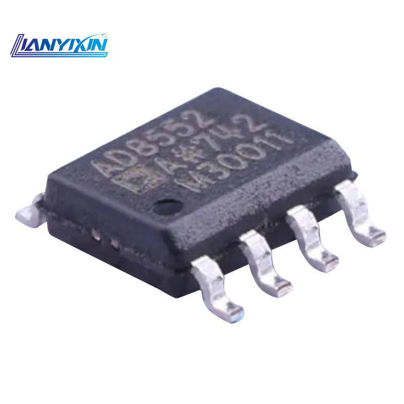
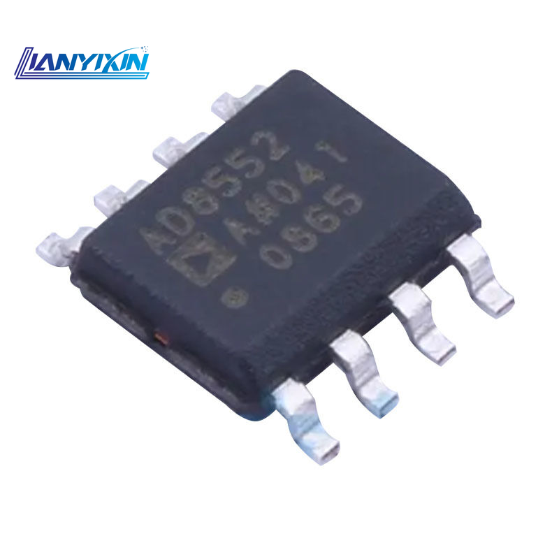
AD8552ARZ-REEL · Analog Devices (ADI) · Circuiti integrati
- Corrente di polarizzazione in ingresso (Ib)
- 160pA
- Tensione di offset in ingresso (Vos)
- 1μV
Prezzo, disponibilità e consegna sono confermati nel preventivo.
Richiedi un preventivoStesso modello · parametri coerenti
| Parametro | Valore |
|---|---|
| Serie | AD8557ARZ-REEL7 |
| Parametro | Valore |
|---|---|
| Numero di amplificatori | Canale singolo |
| Corrente di polarizzazione in ingresso (Ib) | 18nA |
| Tensione di offset in ingresso (Vos) | 2μV |
| Rapporto di reiezione di modo comune (CMRR) | 85dB |
| Corrente di uscita | 25mA |
| Corrente a riposo (Iq) | 1.8mA |
| Alimentazione singola | 2.7V – 5.5V |
| Differenza massima di tensione di alimentazione (Vdd−Vss) | 5.5V |
| Corrente di offset in ingresso (Ios) | 4nA |
| Temperatura operativa | -40°C – +125°C |
| Parametro | Valore |
|---|---|
| Prodotto guadagno-larghezza di banda | 2MHz |
Nessun parametro corrispondente
I parametri si riferiscono a questo modello. Verificare contenitore e condizioni di prova nella scheda del produttore.
Alcuni campi attendono la traduzione e sono riportati separatamente in inglese.
| Product Catalogue | Precision Operational Amplifiers |
|---|---|
| Input Offset Voltage Temperature Drift (Vos TC) | 65nV/℃ |
| Noise Density (eN) | 32nV/√Hz @ 1kHz |
La descrizione localizzata non è ancora disponibile. Di seguito sono riportati i parametri del modello.
Product Overview The AD8557 is a zero-drift sensor signal amplifier featuring digitally programmable gain and output offset capabilities. This amplifier is designed to effortlessly and precisely convert variable pressure sensor and strain bridge outputs into defined output voltage ranges, whilst also accurately amplifying numerous other differential or single-ended sensor outputs. Employing proprietary low-noise auto-zero and DigiTrim technology, the AD8557 delivers a precise and flexible signal processing solution within a compact package. Gain can be digitally programmed over a wide range from 28 to 1300 via a serial data interface. Gain adjustment is fully simulated in-circuit before being permanently programmed using reliable polysilicon fuse technology. The output offset voltage is similarly digitally programmable and proportional to the supply voltage. Beyond its exceptionally low input offset voltage, input offset voltage drift, and extremely high DC and AC common-mode rejection ratios (CMRR), the AD8557 incorporates a pull-up current source at the input pins and a pull-down current source at the VCLAMP pin. Output clamping via an external reference voltage enables the AD8557 to safely and accurately drive low-voltage analogue-to-digital converters (ADCs). When used with an ADC sharing the same supply as the reference, system accuracy remains unaffected by normal supply voltage variations. Output offset voltage adjustment resolution is better than 0.4% of the difference between VDD and VSS. Locking fine-tuning after gain and offset adjustment further ensures field reliability. The AD8557 operates over a temperature range of -40°C to +125°C. This device is powered by a single supply voltage ranging from 2.7 V to 5.5 V and is available in an 8-pin SOIC and a 4 mm × 4 mm, 16-pin LFCSP package. Product Features Ultra-low offset voltage: Maximum 12 μV across the entire temperature range Ultra-low input offset voltage drift: Maximum 65 nV/°C High common-mode rejection ratio: Minimum 96 dB Digitally Programmable Gain and Output Offset Voltage Gain range from 28 to 1300 Compliant with automotive application requirements Single-bus serial interface Stable with any capacitive load SOIC and LFCSP packages Operating voltage range from 2.7 V to 5.5 V Applications Automotive sensors Pressure and position sensors Precision current sensing Thermocouple amplifiers Industrial scales Strain gauges